There are two properties of crystals which are of particular interest to me with regards to semiconductors which calculates the current in a semiconductor and they are:
1. Number of fixed and mobile charges present in the material.
2. The transport of mobile carriers through the semiconductor.
This two properties are the reason why I mentioned crystals in the first place.
Now, conductors have something that is totally opposite to that of semiconductors that I would like to mention and that is its TEMPERATURE COEFFICIENT.
Conductors have a positive temperature coefficient and I am going to explain this for you now.
When I say that conductors have a positive temperature coefficient am only trying to say that an increase in temperature leads to an increase in the resistance of the conductor.
For Example: When I heat a copper rod, the flow of current through that copper rod is reduced.
Therefore, the temperature applied to a conductor is directly proportional to the resistance of the flow of current through that conductor.
The reverse of this occurs in the semiconductors. Semiconductors have a negative temperature coefficient. Just like I explained above this means that an increase in temperature applied to a semiconductor leads to a decrease in resistance.
Silicon is an example of a semiconductor.
So what I am trying to say is that when a silicon is being heated the passage of current through that silicon is increase because the resistance is reduced.
Therefore, the temperature applied to a semiconductor is inversely proportional to the resistance of the semiconductor.
Here is what I understand about semiconductors, Semiconductors are solid materials that behaves as an insulator at absolute zero temperature (0K) and at higher temperatures act as a conductor.
The conductivity of a semiconductor can be greatly increased by the addition of impurities basically known as doping and photoconductivity.
Photoconductivity is process whereby a semiconductor material absorbs light of a certain wavelength to improve its conductivity.
There are two basic types of Semiconductors which are:
1. Element Semiconductors
2. Compound Semiconductors
Element Semiconductors are those conductors that consists of just one element mainly in the group 4 of the periodic table. For Example Silicon (Si), Germanium (Ge) etc.
Compound Semiconductors are those conductors that comprises the combination of two or more elements to form a compound. This is basically the combination of group 3 and group 5 elements like Gallium Arsenide (GaAs) and Indium Phosphide (InP). and the combination of group 2 and group 6 elements like Zinc Sulphide (ZnS) and Cadmium Selenide (CdSe).
As you already know in the world of semiconductors silicon is mostly used that germanium.
Below I outlined some reasons for that:
1. Silicon is abundant in nature therefore, it is readily available and cheap.
2. Silicon is non-toxic and light weight.
3. Silicon forms a better dielectric interface than germanium.
4. Silicon could be operated at higher temperatures than germanium.
5. Silicon forms a stable oxide that is used as a passivation layer during the fabrication of integrated circuits.
Among the compound elements, Gallium Arsenide and Indium Arsenide are the most widely used.
For the production of LEDs, laser diodes, solar cells, microwave integrated circuits etc GaAs is used but it has a setback which is its difficulty to form large diameter rods called ingots that limits the wafer diameter to sizes significantly smaller than silicon.
Lastly, there are two classifications of semiconductor devices which are:
1. Active Semiconductor Devices
2. Passive Semiconductor Devices
The difference between the two is that active semiconductor devices has at least one pn junction while passive semiconductor devices do not have any pn junction.
Examples of active semiconductors are: Transistors, Diodes, Rectifiers etc
Examples of passive semiconductors are: Resistors, Inductors, Capacitors etc.

Intrinsic Semiconductors are those semiconductors that are totally in there pure state. That is they are in a state where there ain't any impurities in it.
Intrinsic Semiconductors can be an element or compound semiconductor.
During conduction in semiconductors electron move to the positive terminal while holes move to the negative terminal. Therefore, current flow in intrinsic semiconductors is due to the movement or motion of thermally generated electrons and holes that move in pairs.
The number of charge carriers per unit volume is known as intrinsic carrier concentration.
ni = N exp(-Eg / 2KbT)
In the above formula:
ni = Intrinsic Carrier Concentration
N = a constant for a given semiconductor
Eg = Energy Gap in Joules
Kb = Boltzmann Constant = 1.38E-38 J/K
T = Temperature in Kelvin
To solve the problem of having a semiconductor with a very large number of electrons moving through positively charged fixed ions or holes we make use of crystalline semiconductors because of their symmetry and order.
Therefore, the electrons move through a well defined periodically arranged distribution instead of random distribution of ions.
Recombination is a process that occurs when an electron loses energy and falls from the conduction band to a hole in the valence band.
Extrinsic Semiconductors are those semiconductors that are doped with controlled amount of impurities.
There are two types of extrinsic semiconductors:
1. n - type semiconductors
2. p - type semiconductors
N - Type Semiconductors are those semiconductors that are doped with a pentavalent (Group 5) element - that is an element that has 5 electrons in its outermost shell.
In the n - type semiconductor, the majority carriers are the electrons while the minority carriers are the holes. Also, the concentration of electrons in the n - type material is far greater than its intrinsic concentration.
Also again, the concentration of holes in an n - type semiconductor is smaller when compared to an intrinsic material because the larger number of electrons present increases the recombination rate.
When pentavalent impurities are added to a semiconductor, an allowable energy level is created just below the conduction band.
P - Type Semiconductors are those semiconductors that are doped with a trivalent (Group 3) element - that is an element that has 3 electrons in its outermost shell.
In the p - type semiconductor, the majority carriers are the holes while the minority carriers are the electrons.
When trivalent impurities are added to the intrinsic semiconductor, an allowable discrete energy level is created just above the valence band.
Under thermal equilibrium, the product of free negative and positive concentration is a constant independent of the amount of donor and acceptor impurity doping. This relationship is known as Mass Action Law.
Equation for Mass Action Law : np = ni2

Fermi level is the top of the collection of electron energy level at absolute zero temperature (0K).
Fermi Energy is the maximum energy possessed by any electron at absolute zero temperature (0K).
F(E) = 1/(1 + e^((E - Ef)/KT))
F(E) has a 50% probability,
Tere are two conditions when T = 0K
1. If E >> Ef, the exponential term becomes finite and F(E) = 0. This implies that there is no probability of finding an occupied quantum state greater than Ef at absolute zero.
2. If E << Ef, the exponential term becomes 0 and F(E) = 1. This implies that all quantum levels with energies less than Ef will be occupied at T = 0K.
Fermi Level in Semiconductors
At room temperature KT = 0.03eV
If E - Ef >> 0.03, F(E) = 0
if E - Ef << 0.03, F(E) = 1
This implies that at room temperature some electrons are excited to higher energies and some states near the bottom of the conduction band Ec will be filled. Similarly near the top of the valence band Ev the propability of occupancy is decreased from unity since some electrons have escaped from their covalent bond and are now in the conduction band.
Fermi Level in a Doped Semiconductor

If a donor type impurity is added to the crystal, the fermi level will move closer to the conduction band. If an acceptor type impurity is added to the crystal, the fermi level will move closer to the valence band.
Since Bohr's postulates is still in use I would like to state them below:
1. Electrons can move only in certain permitted orbits.
2. The energy of an electron in a particular orbit is definite.
3. Each permitted orbit is associated with a level of energy.
4. Atoms radiate out only when an electron jumps from one orbit to another.
5. If E2 and E1 are the energies corresponding to two orbits before and after the jump the frequency of the emitted photon is given by: hf = E2 - E1.
According to Bohr's model, centrifugal force acting on the revolving electron must balance the electrostatic pull by the positively charged nucleus.
Equation: mv2 / r = ze2 / 4πε0r2
Furthermore, their angular momentum can only have integral multiples of a certain value
Equation: mvr = nh / 2π
Eliminating r from the two equations, the orbital radius is:
rn = ε0n2h2 / πmZe2
where:
Z = Atomic Number
ε0 = Permittivity of free space
e = Charge on an Electron
m = Mass of an Electron
h = Planck's Constant
n = Principal Quantum Number
The radii of the permitted orbit vary as the square of the principal quantum number.
The velocity of electrons can be found and it is inversely proportional to orbital radius. This implies that the electron in the innermost orbit has the highest velocity
There are two types of electron energy:
1. Kinetic Electron Energy
2. Potential Electron Energy
Equation of Kinetic Electron Energy = Ze2 / 8πε0r
Equation of Potential Electron Energy = -Ze2 / 4πε0r
The orbital energy is the sum of the potential electron energy and the kinetic electron energy.
Equation of the Orbital Electron Energy = -mZ2e4 / 8ε02n²h²
Electron energy is inversely proportional to the square of the principal quantum number.
The drawing of horizontal lines to an energy scale is known as energy level diagram.
A group of sub orbits is known as shell.
Azimuthal quantum number helps to determine the shape of different sub shells (circular or elliptical).
Pauli's Exclusion Principle states that no two electrons in an atom should have the same sets of values for its four quantum numbers.
Pauli's exclusion principle does not allow the electron energy levels to be the same so that one obtains a set of closely spaced energy levels forming an energy band.
Principal quantum number determines the size of the orbital.
If an electron jumps to an inner energy level, a photon (that is a quantum of electromagnetic energy) will be emitted. The valence band is highest occupied band

Pauli's Exclusion Principle
In semiconductor device fabrication, contaminants are specified by the number of particles per cubic meter for a given particle size.
The various semiconductor device fabrication processes fall into five general categories:
1. Wafer Manufacturing
2. Oxidation
3. Lithography
4. Diffusion
5. Packaging

A Silicon Wafer
The starting material for manufacturing microelectronic devices is pure mono crystalline silicon ingots but for IC fabrication Semiconductor Grade Silicon is used as the starting material.
In wafer manufacturing, trichlorosilane is dominantly used for the following reasons:
1. It can be easily formed by the reaction of anhydrous hydrogen chloride at low temperature. (200°C - 400°C).
2. It is liquid at room temperature. Therefore, distillation can be easily carried out.
3. It can be deposited on heated silicon.
4. It reacts at low temperature and at faster rates than SiCl4.
The hydrogen reduction of trichlorosilane on heated silicon rod is called Siemens method.
Equation: SiHCL3 + H2 => Si + 3HCL
Disadvantages of Siemens Method are:
1. High Power Consumption
2. Poor Silicon and Chlorine Efficiency
Granular Polysilicon Deposition uses the decomposition of monosilane in a fludized bed deposition reactor to produce free flowing granular polysilicon.
Equation: SiH4 => Si + 2H2
Because of the large surface area, fluidized bed reactor are much more efficient than the siemens type rod reactor.
Merits of Using Fluidized Bed Reactor are:
1. It is highly efficient.
2. It is a closed loop and green process.
3. It is easier to melt for the next process of growing monocrystals.
There are two techniques for the production of monocrystalline silicon which are:
1. Float Zone Method
2. Czochralski Method
The float zone method uses an induction heating radio frequency coil to melt the polysilicon rod. A seed crystal with the desired orientation is held by a rotating rod placed just below the polysilicon rod and as the heater traverses the polysilicon rod, it moves with the molten zone, as the tip of the molten zone touches the rotating seed crystal it solidifies (freezes).
A monocrystalline rod grows an extension of the seed crystal as the seed crystal is being withdrawn. In the presence of any impurities or dislocation in the polysilicon they are drawn to the neck and cut off at the end of the process.

Float Zone and Czochralski Method
The Czochralski method involves three steps which are:
1. Melting Polysilicon
2. Seeding
3. Growing
In the Czochralski method, polysilicon chunks are filled in a quartz crucible and melted at temperatures higher than 1420°C in an inert gas or vacuum for a while to ensure complete melting and ejection of air bubbles.
Seeding then takes place where a monocrystalline seed crystal installed in a shaft is dipped into the melt until it begins to melt itself, the melt temperature is lowered until a small amount of crystalline material is solidified.
Growth then takes place, in this case the seed is gradually withdrawn from the melt and once the proper diameter is achieved the seed lift is increased.
Towards the end, the crystal diameter is gradually reduced to form an end cone. When the diameter becomes small enough, the crystal can be separated from the melt without the generation of dislocations
Once the growth process is complete, the crystal is cooled inside the furnace for up to 7 hours to stablize and ensure easier handling.

The float zone silicon crystal has a higher purity than the Czochralski silicon crystal but the Czochralski silicon crystal has a higher mechanical strength than the float zone seed crystal.
Also note that the Czochralski silicon crystals are cheaper and has larger diameters.
With monocrystalline silicon ingot as the starting material, the processes involved are:
1. Trimming and Orientation
2. Flattening
3. Ingot Etching
4. Slicing
5. Edge Rounding and Lapping
6. Slice Etching
7. Polishing and Cleaning
Primary flat is used to correctly align the wafer during device fabrication while secondary flat is used to identify wafer plane orientation and conductive type.
Polishing has two process which are:
1. Mechanical (to create flatness)
2. Chemical (to create smoothness)
Contaminants of a wafer are categorized into three which are:
1. Molecular Eg. resins, oils skin which are held to the wafer by weak electrostatic force.
2. Ionic Eg: Na+, F-, I- which can be removed by chemical reaction
3. Atomic Eg: Au, Fe, transition metals which can be removed by chemical reagents.
Water - Hydrogen Peroxide - Ammonium Hydroxide is the compound for chemically cleaning organic contaminants
Water - Hydrogen Peroxide - Hydrogen Chloride is the compound for chemically cleaning alkali and transition metals.
The purpose of epitaxy is to grow a silicon layer of uniform thickness and accurately controlled electrical properties that will provide a perfect wafer substrate for the subsequent device processing.
All the individual microelectronic circuits and components are fabricated in the epitaxial layer while the p - type substrate supports the epitaxial layer and electrically isolates the circuits from each other.
Silicon epitaxy is done to improve the performance of bipolar devices.

Disadvantages of Epitaxy:
1. Higher cost of wafer fabrication
2. Additional process complexities
3. Problems associated with defects in the epitaxial layer.
There are three types of epitaxial processes that I know of which are:
1. Vapour Phase Epitaxy
2. Molecular Beam Epitaxy
3. Liquid Phase Epitaxy
Vapour Phase Epitaxy
This is an epitaxial process whereby reduction of silicon tetrachloride is carried out in a horizontal tube reactor. Clean wafer substrates is placed on the graphite susceptor in the reactor and silicon tetrachloride vapour with hydrogen is passed over the wafers at very high temperature (1200°C).
Equation : SiCl4 + 2H2 => Si + 4HCl
The growth rate depends strongly upon the proportion of the two source gases. Growth rates above 2 micrometer per minute produce polycrystalline silicon and etching may occur.
Liquid Phase Epitaxy
This epitaxial process deposits a monocrystalline film from the liquid phase, typically at a rate of 0.1 to 1 micrometer per minute. The process occurs at temperatures well below the melting point of the deposited semiconductor. The semiconductor is then dissolved in the melt of another material. At conditions that are close to the equilibrium, semiconductor crystal is deposited on the substrate.
The equilibrium condition depends on the temperature and the concentration of the dissolved semiconductor in the melt.
The growth of the layer from the liquid phase can be controlled by a fixed cooling of the melt.
This process is mainly used for the growth of compound semiconductors, also very thin, uniform and high quality layers can be produced.
The epitaxial layer usually has a different doping concentration from the substrate. The core of an epitaxial reactor is the reaction chamber, typically made of quartz. Inside the chamber is the susceptor, a holder for the silicon substrate typically made of graphite coated with silicon carbide.
The susceptor provides two things which are:
1. Mechanical support for the wafers
2. An environment with uniform thermal distribution

Four Point Probe
This is a method commonly used to measure the sheet resistance of epitaxial layers.
Limitations of Four Point Probe Method
1. The probes must be able to make ohmic contact with the material and GaAs cannot be probed that way.
2. Very low resistive material requires the maximum current from the current source to achieve a reading on display.
3. Only very thin films can be measured --- The current through the probe is best restricted to 10mA because of heating effects and excessive current density at the probe tips.
4. Low level measurements are negatively affected by various sources.
5. High sheet resistivity material can be measured using very low currents and avoiding a greater voltage indication than 200mV.
Microelectronic circuit components are formed by diffusion of impurities into the epitaxial layer.
Areas over which a particular diffusion is required are defined by an oxide layer with windows cut in it.
Areas with oxide inhibit diffusion while areas without allow impurities to diffuse through it.
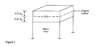
The oxide used for masking diffusion is usually silicon dioxide.
Besides, the use of silicon dioxide as a diffusion barrier for selecting doping silicon. Other uses of silicon dioxide include:
1. Dielectric (insulator) for MOS devices.
2. Passivation and Protection of the silicon wafers.
For oxidation, cleanliness is targeted to the molecular level.
The RCA clean is implemented before oxidation to remove the following:
1. Organic Contaminants
2. Trace Metals
3. Alkali Ions
Silicon wafers are oxidized by placing them in a high temperature furnace (900°C < T < 1200°C) in the presence of oxygen or water.
By controlling temperature and oxidation time precisely, oxide thickness can be predicted and controlled accurately.
There are two types of oxidation which are:
1. Dry Oxidation (1000°C - 1200°C) Equation : Si + O2 => SiO2 + siH2
2. Wet Oxidation (900°C - 1000°C) Equation: Si + 2H2O => SiO2 + 2H2
Mathematical modeling has shown that the relationship for long oxide time is parabolic while for short oxide time, the oxide thickness versus temperature is linear.
For long oxidation times, the process may be modeled by a simple equation known as the parabolic growth law which is x02 = Bt
where:
x0 = Thickness of the growing oxide
B = Parabolic Rate Constant
t = Oxidation Time
Short oxidation times can be modeled by another simple equation known as the linear growth law which is x0 = C(t + λ)
where:
C = Linear rate constant
t = Oxidation Time
λ = Initial time displacement to account for the formation of the initial oxide layer at the start of the oxidation process.
Factors that influence oxide growth:
1. Temperature: The growth rate of the oxide increase with the temperature
2. Moisture: Silicon dioxide grows better in steam because water has a much higher solubility than dry oxygen in silicon dioxide. Thus, water vapour or steam makes thicker oxide. When a thin oxide is needed dry oxygen is used.
3. Duration: The thickness of the oxide increases with time.
4. Crystal Orientation
5. Pressure
Photolithography is the process of transferring the window pattern (geometric shapes) on a mask to the wafer surface.
This shapes make up parts of the circuit in (bases, emitters, collectors) bipolar and (gates, sources, drains) MOS (metallic oxide semiconductor) transistors.
The final IC is made by essentially transferring the features from each mask level to the surface of the silicon.
Steps/Key of Photolithographic Processes
1. Obtain Clean Water
2. Coat water with photoresist
3. Soft Bake
4. Align Mask
5. Expose Patterns
6. Develop Photoresist
7. Hard Bake
8. Etch Windows
9. Strip Photoresist
It is good to use clean materials and work in a clean environment because any dust particle on the wafer constitutes a defect which will eventually result in the failure of the circuit.
Soft baking (150C) of the wafer is done in a safe yellow light.
Selective Oxide Etching
In this process, the photo resist coated wafer is placed into a hydrofluoric acid bath to remove the exposed oxide.
The hydrofluoric acid will react chemically with the oxide to form wafer soluble products that dissolve in the water used to dilute the acid.

In negative photoresist emulsion, Hydroflouric acid is used since it does not react with silicon. Subsequently, the remaining hardened photoresist is finally 'stripped' with a mixture of sulphuric acid and hydrogen peroxide. A final wash and dry stage completes the photolithographic process.
Positive photoresists emulsion behaves in the same manner except that windows are opened where the mask is transparent. They are useful when large areas of oxide is transparent.
Photolithography has limitations as regards the minimum line widths and feature sizes of microelectronic devices that can be fabricated.
An alternative to photolithography is the patterning of the wafer directly without masks. In this technique, the wafers are coated with electron resists then direct writing with electron beam machine is used.
Electron beam machining of masks can produce very fine patterns with high resolution thus the mask can be produced by directly eliminating the photo reduction stages.
Advantages of Direct Writing with Electron Beam are:
1. Fine Patterns
2. Higher Reliability and Resolutions
Disadvantage of Direct Writing with Electron Beam is:
1. It is more expensive.
The main objective of diffusion is to change the type and level of conductivity of semiconductor materials so as to form bases, emitters and collectors of bipolar junction transistor and gates, sources and drains of metallic oxide semiconductor devices.
Diffusion is also used to dope polysilicon materials to form resistors and interconnects.
There are two types of diffusion which are:
1. Substitutional Diffusion: This is a type of diffusion whereby impurity atoms diffuse by moving from a lattice site to a neighbouring one by substituting for a silicon atom which has vacated a usually occupied site.

2. Interstitial Diffusion: This is a type of diffusion whereby heavy metal ions occupy the interstitial voids present in silicon lattice. It helps to reduce carrier lifetimes.

Diffusion depends on the following:
1. Lattice Environment
2. Geometry of Parent Semiconductor
3. Concentration of Gradient of Impurities
4. Physical Properties of a Particular Impurity
Fick's First Law
This is an equation describing the flow of an impurity into a substance showing that the flux of the material across a given plane is proportional to the concentration gradient across the plane.
Equation: J = -D∂N(x, t) / ∂x
The negative sign shows that the flow is in the direction of decreasing concentration.
From the equation:
N = Density of Concentration of Impurities
D = Diffusion Coefficient
∂N/∂x = Concentration Gradient
x = Co-ordinate axis in the direction of impurity flow
t = Diffusion Time
Fick's first law is not an adequate description of the diffusion process since the concentration gradient of an impurity in a finite volume of material decreases with time.
Fick's Second Law
From the conservation of matter, this law states that the change in impurity concentration over time is equal to the change in local decrease of diffusion flux.
Equation: ∂N(x, t)/∂t = -∂J(x, t)/∂x
There are two types of boundary conditions for modeling impurity diffusion in silicon which are:
1. Constant - Source Diffusion: This is a boundary condition whereby the surface concentration is held constant throughout the diffusion.
2. Limited - Source Diffusion: This is a boundary condition whereby a fixed quantity of the impurity is deposited on a thin layer on the surface of the silicon.
Planar Diffusion From a Constant Source of Dopants
In planar type of diffusion, dopants are deposited or introduced on to the surface of a hot silicon slice.
The dopants are allowed to diffuse into the material whereas the amount of dopant at the surface is being maintained at a constant level throughtout the diffusion.
This type of diffusion is called complementary error function diffusion.
Therefore, a constant source results in a complementary error function impurity distribution.
As time progresses, the diffusion proceeds further into the wafer with the surface concentration remaining constant.
The total number of impurities atoms per unit area in the silicon is called DOSE, Q (atoms/cm²).
The dose is directly proportional with time (Q increases with time) and an external impurity source must supply a continuous flow of impurity atoms to the surface of the wafer.
In constant source diffusion, there is a high surface concentration and for this reason it is used for emitter type diffusion.
Two - Step Diffusion
This is a diffusion whereby the impurity concentration and profile can be carefully controlled.
In step one, the deposition stage, a constant source diffusion is carried out for a short time usually at a relatively lower temperature (1000°C).
In step two, the drive-in stage, the impurity supply is shut off and the existing dopant is allowed to diffuse onto the body of the semiconductor which is now held at a higher temperature (1200°C) in an oxidizing atmosphere.
The oxide layer which is formed during this stage prevents impurities from entering and the ones deposited from diffusing out.

The final impurity profile is a function of factors such as temperature, time and diffusion coefficient for each step.
Junction Formation
The goal of most diffusions is to form pn junctions by converting p - type material to n - type material or vice versa.
The point at which the diffused impurity profile intersects the background concentration is the metallurgical junction depth.
The net impurity concentration at the metallurgical junction depth is zero. The material to the left of the metallurgical junction depth is the p - type while to the right is the n - type.
Diffusion of dopants is carried out in electric furnace tubes using solid, liquid or gaseous sources.
In a solid source doping system, carrier gases (N2 or O2) flow at a controlled rate over a source boat placed in the furnace tube. The carrier gases picks up vapour from the source and transports it down the tube where dopant is deposited on the wafer. Solid Boron and Phosphorus impurity sources are available in wafer form and are placed in a quartz boat in the furnace.
In liquid source systems, a carrier gas passes through a bubble where it picks up the vapour of the liquid source. The gas carries the vapour into the furnace tube where it reacts with the surface of the silicon wafer.
In gas source systems, the dopants are supplied directly to the furnace tube in the gaseous state.
Note that common gas sources are toxic and purging, trapping systems are used to ensure that all the source gas is removed from the furnace before wafer removal.
Commonly used p - type dopants used for p - type diffusion is boron. Gallium and Aluminium are not used because they have a very high diffusion coefficient in silicon dioxide, Indium is also not used because it does not produce holes easily at room temperature.
Equations:
Solid Source of Boron: 2B2O3 + 3Si <=> 4B + 3SiO2
Liquid Source of Boron: 4BBr3 + 3O2 => 2B2O3 + 6Br2
Gaseous Source of Boron: B2H6 + 3O2 => B2O3 + 3H2O
Commonly used n - type dopants used for n - type diffusion are antimony, phosphorus and arsenic
Equation:
Solid State of Phosphorus: 2P2O5 + 5Si => 4P + 5SiO2
Gold is often diffused into silicon wafers to enhance the recombination rate and so increase the switching speed of active devices.
Ion Implantation is another method of introducing dopants into silicon besides chemical deposition by solid state diffusion.
It involves introduction of ionized projectile atoms into targets. Such atoms are given enough energy to penetrate beyond surface regions. The depth of implantation which is proportional to the ion energy can be selected to meet any particular application.
The two key parameters that define the final implant profile are:
1. Dose
2. Energy
The dose is related to the beam current, I where Q = It / qiA
Where:
t = Implantation Time
A = Beam Area
qi = Charge per ion

The major advantage of ion implantation is the ability of precisely controlling the number of dopant atoms and the depth of penetration.
It has a setback which is the slight destruction of the surface of the slice which is corrected by thermal annealing (heating to a very high temperature, 500°C - 1000°C).
In comparison with chemical deposition, ion implantation is clean and dry because it is performed in a vacuum.
Another advantage of ion implantation is that masks can be made of any convenient material such as photoresist, oxides, nitrides etc.
Ion Implantation System
This consists of ion source where ions of desired elements are produced. An accelerator where electrons are electrically accelerated to a high energy and a target chamber where the ions impinge on a target which is the material to be implanted.
Each ion is a single atom and thus the actual amount of the material to be implanted ie the dose is the integral over time of the ion current.
The energy of the ions as well as the type of ion and the composition of target determine the depth of penetration of the ions in the solid.

In metallization, metal films are used for interconnecting the components to form an integrated circuit.
After all diffusion and oxidation steps are completed, metal is deposited onto the surface of the wafer to 'wire' the device fabricated in the silicon together.
The metallization process involves putting the wafer into a large chamber and pumping air out of the system.
For Example: A piece of aluminium located on a tungsten 'boat' in the system is heated to high temperature, causing the aluminium to melt and evaporate. The evaporated aluminium will solidify into a thin film when it touches the silicon wafer.
After metallization, the wafer is completely covered by the aluminium. The wafer must be patterned and etched to form the actual 'wires' connecting individual devices into a circuit.
The wafer is covered with silicon dioxide, the various metal layers are interconnected by etching holes called 'vias' and depositing tungsten in them. Other metals besides aluminium can be used too.
Wafer Testing
The equipment for wafer testing marks each bad chip with a drop of dye. The proportion of the devices on the wafer found to perform properly is referred to as yield. The wafer with low yield are discarded because it has many bad chips.

Steps before a chip becomes usable are:
1. Wafer Dicing
2. Die Attach
3. Wire Bonding
4. Encapsulation
5. Branding
Wafer Dicing
This is the breaking down of good wafers into individual chips. Dyed chips are thrown away because they are no longer useful while the undyed ones are packaged.
Die Attach
This is the putting of die attach material such as silver filled epoxy or silver filled parts on the die pad by the use die attach equipments like die bonders using epoxy dispensing tools.
Wire Bonding
This is the provision of electrical connection between the silicon chip and the external leads of the semiconductor device using very fine bonding wires.
Encapsulation
This is the sealing of the package in a sealing furnace
Branding
This is the process of applying identification marks on the package.
Note that in the final testing of the chips two test are involved which are:
1. Parametric Testing: This checks if the device exhibits the correct voltage, current or power characteristics regardless of whether the unit is functional or not.
2. Functional Testing: This checks if the device is able to perform its basic operation.
Chips that fail these tests do not scale through.
2 Photos Culled From: Introduction to Semiconductor Devices Technology by Prof. Mrs Gloria Chukwudebe
No comments:
Post a Comment