In a JFET, the current conduction is either by electrons or holes and is controlled by means of an electric field between the gate electrode and the conducting channel of the device.
Note that the JFET has a high input impedance and a low noise level (because there are no junctions as in an ordinary transistor, conduction is through an n - type or p - type semiconductor material).

The three terminals of a JFET are:
1. Gate
2. Drain
3. Source
The voltage betwee the gate and the source is such that the gate is reverse biased and the drain and source terminals are interchangeable
It is worthy to note the following points:
1. The input circuit (gate to source) of a JFET is reversed biased which means that the JFET has a high input impedance.
2. The drain is so biased with the source that the drain current ID flows from the source to drain.
3. In all JFETs, source current IS is equal to the drain current ID.
4. The input voltage (VGS) controls the output current.
5. JFET is not subjected to thermal runaway when temperature increases, the drain current (ID) is controlled by the changing channel width.
Working Principle of a Junction Field Effect Transistor (JFET)

The two pn junctions at the sides of a JFET form the two depletion layers and the conduction by charge carriers (ie free electrons because we are dealing with n - channel JFET) is through the channel between the two depletion layers and out of drain.
The width and hence the resistance of this channel can be controlled by changing the input voltage, VGS. The greater the reverse voltage VGS, the wider the depletion layers and the narrower the conduction channel.
The narrower the conduction channel means greater resistance and hence source to drain current decreases while the wider the conduction channel means lesser resistance and hence source to drain current increases.
Therefore, the JFET operates on the principle that width and hence resistance of the conducting channel can be varied by changing the reverse voltage, VGS.
In other words, the magnitude of the drain current, ID can be changed by altering VGS.
When a voltage, VDS is applied between drain and source terminals and voltage on the gate is zero, the two pn junctions at the sides of the bar establishes depletion layers. The electrons will flow from source to drain through a channel between the depletion layers. The size of these layers determines the width of the channel and hence the current conduction through the bar.
If the reverse voltage, VGS is continuously increased, a state is reached when two depletion layers touch each other and the channel is cut off. Under such conditions, the channel becomes a non conductor (insulator).
Differences Between JFET (Junction Field Effect Transistor) and BJT (Bipolar Junction Transistor)
JFET
1. Unipolar transistor
2. Voltage controlled device
3. Its terminals are gate, source and drain
4. Its input circuit is reverse biased
5. It has a high input impedance
6. No current enters the gate of a JFET
7. Noise level is very small
8. Its gain is characterised by transconductance which is ratio of change in output current (ID) to input voltage (VGS).
BJT
1. Bipolar transistor
2. Current controlled device
3. Its terminals are emitter, base and collector
4. Its input circuit is forward biased
5. It has a low input impedance
6. Few currents enter into the base of a BJT
7. Noise level is moderate
8. Its gain is characterised by current gain
The curve between the drain current (ID) and drain source voltage (VDS) of a JFET at constant gate source voltage (VGS) is known as the output characteristics of a JFET.

Note that at first, the drain current (ID) rises rapidly with the drain source voltage (VDS) but then becomes constant. The drain source voltage above which the drain current becomes constant is known as PINCH OFF VOLTAGE.
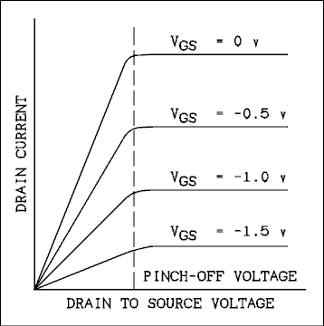
After pinch off voltage the channel width becomes so narrow that depletion layers almost touch each other and the drain current passes through the small passage between these layers. Thus, increase in drain current is very small with VDS above pinch off voltage. Consequently the drain current (ID) remains constant.
No comments:
Post a Comment